Wiegand Converter
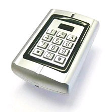
Description
The common RFID reader and keypad for access control uses the Wiegand standard to communicate with the rest of the electronic entry system. Due to its ability to transmit over long distance and simple interface it is widely used in the security industry. This tutorial will describe the Wiegand physical interface, the Wiegand protocol, specifically the EM 26bit version and how the MonkeyBUS is used to read the data. This example can also work for other variation and implementation of the Wiegand protocol with minor alteration at software level.
Features
- Convert 26 bit Wiegand code to keyboard input
- Shows the raw Wiegand code, facility code and card/key ID
- LED indicating a Wiegand is read
- Bootloader
Hardware
The Wiegand physical layer uses three wires
- common ground
- Data 0
- Data 1
Data 0 and Data 1 are also known as Data Low and Data High respectively. When the data lines are idle, the lines are at logical high, normally at +5V. When binary 0 is being sent, Data 0 (data low) wire will move from high to low whilst Data 1 (data high) will remain high. When binary 1 is being sent, Data 1 (data high) will move from high to low whilst Data 0 (data low) will remain high. The distance between the Wiegand device and the access control panel should be less than 150 meters.
To capture the data using the MonkeyBUS, the data lines are directly connected to the MonkeyBUS's interrupt pins. Whenever Data 0 is toggled, the software will add a binary 0 to the Wiegand number and whenever Data 1 is toggle, a binary 1 is added to the Wiegand number. The software will detect the end of transmission and calculates the final result.
The MonkeyBus acts as keyboard HID when plugged into a USB port of a Windows machine. Data 0 and Data 1 of the Wiegand output connect directly to pin 2 and pin 4 of JP2 on the MonkeyBus. Due to variety of Wiegand device, it is recommended Wiegand device to be powered by external power supply. However, the MonkeyBus can wire up in such a way that both of MonkeyBus and Wiegand devices can be powered by the USB port if the Wiegand device can be powered by 5VDC and the current requirement is lower than the standard USB current supply. The wiring diagram is example of a wireup for a standard Wiegand device using external power supply.
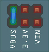
Set the jummper switch to VBUS to power on the MonkeyBUS.
Wire up the Wiegand device.
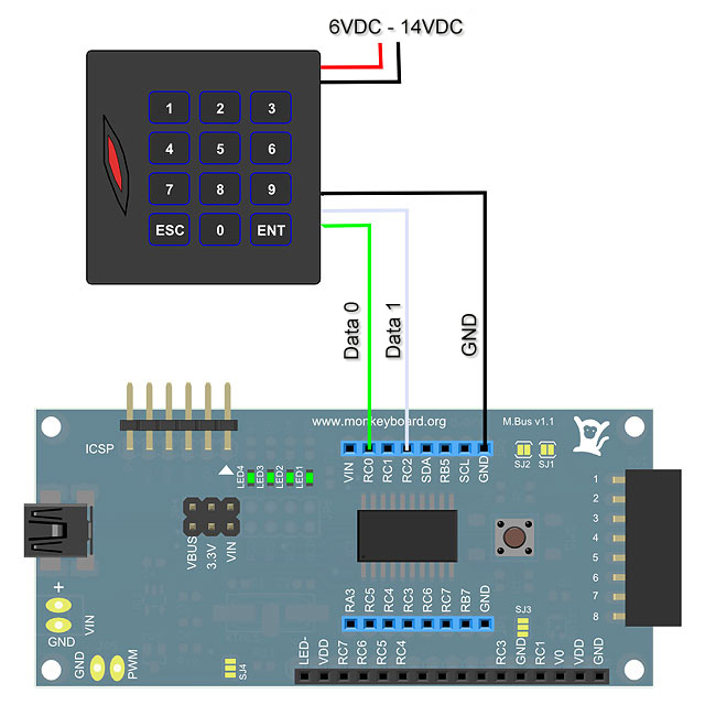
The hardware setup is complete, its ready to be flash with sosftware.
Software
As mentioned earlier, the Data 0 and Data 1 triggers an interrupt. The interrupt service routine aggregate the 0s and 1s from Data 0 and Data 1 line and stores it in a temporary variable. To accommodate other variation and implementation of RFID (for example 34 bit Wiegand from HID), the software will wait for a period of time after the data lines are idle before assuming the end of transmission.
Most 26 bit EM Wiegand devices, which have 24 bits of data, emit 8 bits facility code and 16 bits ID code after leading parity bit. The first parity bit is calculated from the 12 most significant bits and the trailing parity bit from the 12 less significant bits. Since Wiegand is so widely used and customised, some vendors might have their own data scheme even though Wiegand is used as the transmission medium.
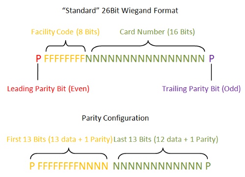
Diagram shows an example of standard 26 bits Wiegand protocol
The MonkeyBUS software does the following:
- Wait for interrupt
- Collect data from GPIO
- Wait for timer to expire
- Send information via HI USB controller
To break it down in to components, MonkeyBus software utilises the following PIC18 features:
- GPIO and GPIO Interrupt
- Timer and timer interrupt
- HID USB controller
- Wiegand interpretation
General Purpose Output
UserInit() function is where GPIO setup is done. The LED indicators in port C (RC1 and RC3) are set as outputs by the macro mInitAllLEDs which modifies the registers:
TRISC (TRI-STATE REGISTER)
LATC (DATA LATCH REGISTER)
The bits in TRISC is memory mapped to port C pins, that is to say TRISC0 correspond to RC0. So bit 1 and 3 are set
TRISC &= 0xF5;
Similarly, the latch registers to latch outputs
LATC &= 0xF5;
At list of macro to set, clear or toggle LED pins can be found in HardwareProfile - Low Pin Count USB Development Kit.h
General Purpose Input
The PIC18 treats input as analogue. Therefore,
ANSEL=0
register is clear to ensure they treated as digital inputs.
RC0 and RC2 are used to receive data from data0 and data1 line respectively from the Wiegand device. An interrupt service routine is used to process data bits into Wiegand code. A sample of the actual pulse is shown below. To capture the pulses, the input pin is set to trigger on a falling edge
INTEDG0=0
and enable the interrupt by
INT0IE=1
The same configuration applies for INT2.
The interrupt flag is the cleared ready for the next interrupt to trigger. mClrInt0F clears the INT0IF register. The following steps summarise input setup:
- Set negative trigger using INTEDGx register
- Set interrupt enable setting INTxIE register
- Clear interrupt flag ready for next trigger by clearing INTxIF register
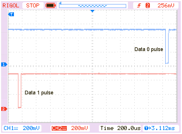
Diagram shows relationship between Data 0 and Data 1 pulses. Note that some Wiegand devices have 50us low pulse and some have 100-200us low pulse.
Timer
A timer is required to note an end to a transmission. The main program loop will wait for 25ms from the last pulse before processing the data. To do this a tick counter increments every 1ms by its interrupt. The input interrupt routine stores the time the last bit was received. All the main loop has to do is to find the difference between the two times.
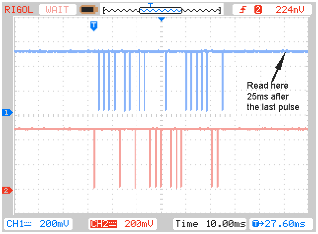
An example of data captured, 10000100100111011100000110, after removing the leading and trailing parity, the data is 000010010011101110000011, and equals to 0x93B83.
Timer Setup
The mTimer0Con sets timer 0 to a 16 bits counter, enables timer zero, set prescaler multiplier and use internal clock. The timer interrupt will trigger when an overflow occurs. To calculate the preload value, use the formular:

In this example, the prescale is set to 4 and for 1000 ticks per second, the above formula yield the preload value 0xF448.
After setting up everything, make sure global interrupt is enabled by setting GIE.
HID USB controller
The Microchip example where this application is based on has the HID and USB stack already implemented. The USB task USBDeviceTasks is polled in the main loop. The Keyboard routine will pump the character to USB as a keyboard input. The Wiegand interpreter modify this a little bit by adding the line
while (HIDTxHandleBusy(lastINTransmission));
to make sure transmission is complete before moving on to the next character. The characters are mapped to keyboard input by the keyLookup array. If more characters are needed add them to the array or add the CheckAscii switch cases.
Interpreting Wiegand
An interrupt routine will run each time the data lines are triggered by negative edge. All the routine is doing is to shift a variable by 1 bit and wait for the next trigger. When the interval between bits is greater than 25ms, the main loop assumes a read is complete and decoding can begin. LED 4 turns on when read is in progress and off when it is complete.
The raw Wiegand code is parsed and send via the USB stack and onto a text editor.
Final Thoughts
This Wiegand interpreter is a simple example demonstrates the following PIC18F14K50 features:
- Timer
- GPIO
- Interrupts
- USB stack
- Keyboard HID
Even though this example is focused on the EM26 bit Wiegand format, other Wiegand variation is very similar, differ only in parity bit calculation and number of total bits transmitted. More examples on the the PIC18 based MonkeyBus can be found on this website.
Downloads
Wiegand to HID Firmware
Wiegand to Serial Firmware


